


WHAT THE TIMELINE IS This timeline explores the history of computing from 1939 to 1994. Each year features illustrated descriptions of significant innovations in hardware and software technology, as well as milestones in areas such as commercial applications and artificial intelligence. When appropriate, biographical sketches of the pioneers responsible for the advances are included. |
The displays were assembled by a coalition of Stanford computer scientists and the Computer History Museum(CHM), formerly the Computer Museum History Center (CMHC), and before that a part of The Computer Museum (TCM) in Boston, has installed exhibits within the Gates Computer Science building containing historical equipment and documents focusing on Stanford's role in the history of computing. The exhibits are being changed and updated as time permits. The first floor exhibit, installed November 1997, focuses on the early history of the Stanford Computer Science Department. and its founder, George Forsythe, and hisstudents. Further exhibits are found on all floors of the building and all can be viewed on-line if you can't make it to Stanford. We are also collecting information about the PhD students, and their students+, that have graduated from the department.
Location
The displays are spread throughout the public areas of the Gates Computer Science building, at Campus Drive and Serra street on the Stanford University campus, Stanford CA 94305-9400.
The current (May 2010) displays are
- Floor 1 Stanford Related Items.
- At the entrance (#8): The Mobi Robot.
- In the Center Lobby (#9): Victor Scheinman's robot arm.
- On the central mushroom, a guide to the various display sites.
- At the far end of the passage (#1): Historical Storage disks
- On the right side above table, left (#2): George Forsythe and students.
- On the right side above table, right (#3): Early Stanford CSD faculty.
- In the table left (#6) Calculators used by Forsythe and Floyd.
- In the table right (#7) Stanford Programming Trophies, Prof. McCarthy's Turing award.
- On the left side, right (#4): Departmental timeline. LOTS.
- On the left side, left (#5): Stanford AI Lab (SAIL) history. More pictures of SAIL participants have been collected; many came from Bruce Baumgartwho maintains a large archive.
- up the left staircase to the second floor, (#6) a new display case showing printing technology; CDC Belt printer, HP laserjet, Linotype slug, printing heads from IBM Selectric, wire printer, daisy wheel printer, inkjet printer, etc.
- up the right staircase to the second floor, (#7) an exhibit of communication technology is under construction: Early Livermore accoustic-coupled modem, Selecterm modem, SAIL asymmetric modem, DECtalk unit, Cisco exhibit, etc;
- In the landing of the stairway to floor 2, a 1969 IBM poster on the history of mathematics.
- location (case umber): Items:
- Side Entrance Planned: Display of the S-1 Mark I computer, a project at Lawrence Livermore Laboratory, involving students and faculty from Stanford(#10).
- Floor 2 In two deep displays (#21-22). Computing in the fifties and earlier.
- Left: Early storage devices: electron-beam tube from SWAC, delay line, RCA selectron tube, Eckert-Mauchly plug-in module. Electric keypunch and cards. In the background Grace Hopper in front of a Univac.
- Right: Whirlwind artifacts: coreplane, logic panel, tube tester; Jay Forester photo.
- In side cabinet (#23): Computing Without Electricity: mechanical integrators, linear and rotary slide rules, log table, Computator, abacus.
- Planned: two boards for explanations (#24-25) next to the alcoves.
- In the landing of the stairway to floor 3, two posters on the History of Computers (to 1967) [British] and History of Microprocessors.
- Floor 3 In two deep displays (#31-32). Computing in the sixties.
- Left: IBM 360 artifacts: 360-65 9020 (FAA special) front panel, core panels, manuals.
- Right: DEC PDP-6 artifacts and modems. Picture of Gordon Bell's group. DEC cartridge disk, Model 33 Teletype, punched paper tape.
Planned: Timesharing technology. - In side cabinet(#33): CROMENCO computing with a C-3 system, terminal, camera, posters, 8" floppy drive, Roger Melen and Harry Garland book, manuals.
- Planned: two boards for explanations, next to the alcoves: (#34),
- Stanford Computer Systems History, (#35) timesharing
- In the landing of the stairway to floor 4, Language History, Silicon Valley History posters.
- Floor 4 In two deep displays (#41-42).
- Right: Early personal computers: Apple, Pet, Commodore, Osborne portable.
- Left: Sun computers: First working board, Early SUN, disk drive. Photos of Andy Bechtolsheim, Scott McNealy, Bill Joy, Vinod Khosla, Laura Tong, and Vaughan Pratt.
- Side cabinet (#43): Apple display, in preparation.
- Computing in the seventies and later.
- Floor 5
- Card Cabinet (#51) The manuscript on punched cards and generating programs for David Gries' Compiler Construction for Digital Computers; John Wiley and Sons, New York, 1971, 491 pages.
- Wall cabinet (#52) Two copies of David Gries' Compiler book, one opened to show the metal typefont avialble then.
Now removed to the CMHC: The original 1971 Galaxy Star Wars computer game. (A Web Version).
- Basement floor
- Logic devices, from relay to integrated circuit, with some typical circuit boards.
- Background Election prediction in 1952.
- PDAs and the KBMS group.
- Xerox Altos and mice.
- IBM PC.
- The original Google Storage (#12)
- a wide display (#11) on the wall between the elevators and the HP lecture hall. Computer development timelines (being developed)
Since the ENIAC -- the first computer to be used commercially, went into service in 1945, there have been only three major memory formats.
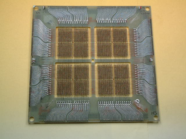
In 1945, the ENIAC computer used thousends of vacuum tubes and had a memory of mercury and nickel wire delay lines. Between 1945 and 1954, delay lines, William tubes and magnetic drums was used as memory devices.
In 1952 at MIT, Jay Forrester invented the Core Memory. A core was a small ring of ferrite, a ferromagnetic ceramic material that could be magnetized in either of two directions. This unique feature of core enabled it to hold a bit of information, either a 1 or 0, depending on the direction of the magnetic charge. Core memory was used in about 95% of all computers by 1976.
READ ONLY MEMORY
The simplest type of solid state ROM is as old as semiconductor technology itself. Combinational logic gates can be joined manually to map n-bit address input onto arbitrary values of m-bit data output (a look-up table). With the invention of the integrated circuit came mask ROM. Mask ROM consists of a grid ofword lines (the address input) and bit lines (the data output), selectively joined together with transistor switches, and can represent an arbitrary look-up table with a regular physical layout and predictablepropagation delay.
In mask ROM, the data is physically encoded in the circuit, so it can only be programmed during fabrication. This leads to a number of serious disadvantages:
- It is only economical to buy mask ROM in large quantities, since users must contract with a foundry to produce a custom design.
- The turnaround time between completing the design for a mask ROM and receiving the finished product is long, for the same reason.
- Mask ROM is impractical for R&D work since designers frequently need to modify the contents of memory as they refine a design.
- If a product is shipped with faulty mask ROM, the only way to fix it is to recall the product and physically replace the ROM.
Subsequent developments have addressed these shortcomings. PROM, invented in 1956, allowed users to program its contents exactly once by physically altering its structure with the application of high-voltage pulses. This addressed problems 1 and 2 above, since a company can simply order a large batch of fresh PROM chips and program them with the desired contents at its designers' convenience. The 1971 invention of EPROM essentially solved problem 3, since EPROM (unlike PROM) can be repeatedly reset to its unprogrammed state by exposure to strong ultraviolet light. EEPROM, invented in 1983, went a long way to solving problem 4, since an EEPROM can be programmed in-place if the containing device provides a means to receive the program contents from an external source (e.g. a personal computer via a serial cable). Flash memory, invented at Toshiba in the mid-1980s, and commercialized in the early 1990s, is a form of EEPROM that makes very efficient use of chip area and can be erased and reprogrammed thousands of times without damage.
All of these technologies improved the flexibility of ROM, but at a significant cost-per-chip, so that in large quantities mask ROM would remain an economical choice for many years. (Decreasing cost of reprogrammable devices had almost eliminated the market for mask ROM by the year 2000.) Furthermore, despite the fact that newer technologies were increasingly less "read-only," most were envisioned only as replacements for the traditional use of mask ROM.
The most recent development is NAND flash, also invented by Toshiba. Its designers explicitly broke from past practice, stating plainly that "the aim of NAND Flash is to replace hard disks,"[1] rather than the traditional use of ROM as a form of non-volatile primary storage. As of 2007, NAND has partially achieved this goal by offering throughput comparable to hard disks, higher tolerance of physical shock, extreme miniaturization (in the form of USB flash drives and tiny microSD memory cards, for example), and much lower power consumption.
No comments:
Post a Comment